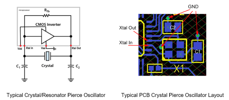
Crystal Printed Circuit Board (PCB) Design Guidelines晶体布线设计指南
![]() Connect the crystal and external load capacitors on the PCB as close as possible to the oscillator input and output pins of the chip.
Connect the crystal and external load capacitors on the PCB as close as possible to the oscillator input and output pins of the chip.
把晶体与其外部负载电容连接到芯片的时钟信号输入和输出引脚,走线越短越好。
 The length of traces in the oscillation circuit should be as short as possible and must not cross other signal lines.
时钟信号电路中的走线长度应尽可能短,且不得与其他信号线交叉。
 Avoid right angle bends on traces
在时钟信号布线时,避免直角弯曲。
 Ensure that the load capacitors CX1, CX2, and CX3, in case of third overtone crystal usage, have a common ground plane.
若使用的为三次泛音晶体,请确保负载电容CX1、CX2和CX3具有共同的接地端。
 Loops must be made as small as possible to minimize the noise coupled in through the PCB, and to reduce any parasitics as much as possible.
尽可能减少环路,以降低噪声及寄生。
 Do not lay out the ground (GND) pattern under crystal unit.
请勿在晶体下方布置接地(GND)线路。
 Do not run Digital / RF signal lines or power under crystal unit for multi-layered PCB.
若为多层PCB板,请不要在晶体下方布置数字线/RF信号线或电源线。


