-
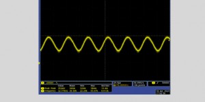; ) 32.768KHz无源晶振应该配多大的电容?
推荐32.768KHz无源晶振两端最好外接15~22PF外接电容,理由如下: 因为32.768KHz晶振本身负载电容一般为12.5PF(其它数值另当别论,如6PF、7PF、9PF等),都没有极性之分,两边的对地电容具体参数要根据电路设计来匹配。 振荡电路都是在一个反相放大器(注意是放大器不是反相器)…时间:2023/03/22
32.768KHz无源晶振应该配多大的电容?
推荐32.768KHz无源晶振两端最好外接15~22PF外接电容,理由如下: 因为32.768KHz晶振本身负载电容一般为12.5PF(其它数值另当别论,如6PF、7PF、9PF等),都没有极性之分,两边的对地电容具体参数要根据电路设计来匹配。 振荡电路都是在一个反相放大器(注意是放大器不是反相器)…时间:2023/03/22
-
; ) 两脚晶振电路使用说明
晶诺威科技生产的两脚晶振产品图如下: 两脚晶振为无源晶振,又被称之为晶体谐振器。一般情况下,在两脚晶振使用时,只要将两脚接在两端,并从两端分别连接一个合适的电容到地线即可。 注: 两脚晶振的两个引脚没有方向性。两脚晶振内部电路图如下所示: 晶振电路由晶振和相关的电容、电阻等元件组成。晶振的频率决定了…时间:2023/03/20
两脚晶振电路使用说明
晶诺威科技生产的两脚晶振产品图如下: 两脚晶振为无源晶振,又被称之为晶体谐振器。一般情况下,在两脚晶振使用时,只要将两脚接在两端,并从两端分别连接一个合适的电容到地线即可。 注: 两脚晶振的两个引脚没有方向性。两脚晶振内部电路图如下所示: 晶振电路由晶振和相关的电容、电阻等元件组成。晶振的频率决定了…时间:2023/03/20 -
; ) 晶振虚焊会导致什么问题?
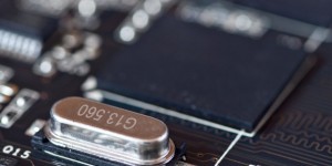
晶振虚焊会导致什么问题? 如果在晶振焊接过程中发生虚焊问题,也就是假焊接,可能导致晶振不通电。“不通电”意味着晶振无法起振或停振,这容易导致我们误判晶振为“不良品”。 另外,在温度升高的情况下,由于热胀冷缩原因,电路板上的晶振引脚虚焊电路可能导通,但在温度降低条件下连接晶振引脚的外部电路再次断开,这…时间:2023/03/16
晶振虚焊会导致什么问题?
晶振虚焊会导致什么问题? 如果在晶振焊接过程中发生虚焊问题,也就是假焊接,可能导致晶振不通电。“不通电”意味着晶振无法起振或停振,这容易导致我们误判晶振为“不良品”。 另外,在温度升高的情况下,由于热胀冷缩原因,电路板上的晶振引脚虚焊电路可能导通,但在温度降低条件下连接晶振引脚的外部电路再次断开,这…时间:2023/03/16 -
; ) 无源晶振没有单片机如何起振?
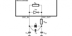
无源晶振没有单片机如何起振? 答:无源晶振无法单独起振。换句话说,无源晶振不接起振电路,是根本无法起振的。 无源晶振起振电路如下: 无源晶振,又名晶体,全称石英晶体谐振器,Crystal,简写为XTAL。双端输出,不需单独供电,起振电路在芯片内部。 有源晶振,全称石英晶体振荡器,Crystal Os…时间:2023/03/08
无源晶振没有单片机如何起振?
无源晶振没有单片机如何起振? 答:无源晶振无法单独起振。换句话说,无源晶振不接起振电路,是根本无法起振的。 无源晶振起振电路如下: 无源晶振,又名晶体,全称石英晶体谐振器,Crystal,简写为XTAL。双端输出,不需单独供电,起振电路在芯片内部。 有源晶振,全称石英晶体振荡器,Crystal Os…时间:2023/03/08 -
; ) 无线麦克风为何需要压控晶振VCXO?
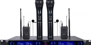
压控振荡器(VCXO)是通过调整控制端电压改变输出频率。一般频率调整范围为±50~±200ppm。改变外加调整电压的大小,能改变容性负载CL的值,从而实现频率的调整。 无线麦克风为RF射频类电子产品,即信号发射端与信号接收端配对工作。其工作原理是: 信号发射端:声音----->电压----->频率 …时间:2023/03/07
无线麦克风为何需要压控晶振VCXO?
压控振荡器(VCXO)是通过调整控制端电压改变输出频率。一般频率调整范围为±50~±200ppm。改变外加调整电压的大小,能改变容性负载CL的值,从而实现频率的调整。 无线麦克风为RF射频类电子产品,即信号发射端与信号接收端配对工作。其工作原理是: 信号发射端:声音----->电压----->频率 …时间:2023/03/07 -
; ) 晶振烧毁的原因是什么?
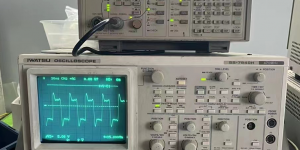
晶振分为两类:无源晶振和有源晶振。根据这两类晶振的内部结构和工作原理的差异,晶振烧坏的情况也应分为两类。 对于无源晶振在以下两种情况下可能被烧坏: 1.手工焊接操作不当 如果采用高温或长时间引导脚部加热,会导致内部石英晶片镀银层破坏、电阻超差等问题,引发晶体不振荡。 2.激励功率过大 根据应用的不同…时间:2023/03/06
晶振烧毁的原因是什么?
晶振分为两类:无源晶振和有源晶振。根据这两类晶振的内部结构和工作原理的差异,晶振烧坏的情况也应分为两类。 对于无源晶振在以下两种情况下可能被烧坏: 1.手工焊接操作不当 如果采用高温或长时间引导脚部加热,会导致内部石英晶片镀银层破坏、电阻超差等问题,引发晶体不振荡。 2.激励功率过大 根据应用的不同…时间:2023/03/06 -
; ) 关于晶振的焊接、清洗及储存的说明
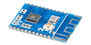
关于晶振的焊接、清洗及储存,说明如下: 1、对于需要剪脚的插件晶振,应该注意机械应力的影响。 2、在晶振焊锡过程中,其焊锡的温度不宜过高,焊锡时间也不宜过长,防止晶体因此发生内变,而产生不稳定。 3、焊锡之后,要进行清洗,以免绝缘电阻不符合要求。不建议使用超声波清洗。 4、晶振外壳需要接地时,应该确…时间:2023/03/04
关于晶振的焊接、清洗及储存的说明
关于晶振的焊接、清洗及储存,说明如下: 1、对于需要剪脚的插件晶振,应该注意机械应力的影响。 2、在晶振焊锡过程中,其焊锡的温度不宜过高,焊锡时间也不宜过长,防止晶体因此发生内变,而产生不稳定。 3、焊锡之后,要进行清洗,以免绝缘电阻不符合要求。不建议使用超声波清洗。 4、晶振外壳需要接地时,应该确…时间:2023/03/04 -
; ) 32.768kHz的无源晶振的等效电容和标称负载电容
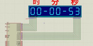
32.768kHz的无源晶振内部没有独立起振电路,需要精准的匹配外部电容才可以输出正确时钟信号。 负载电容(CL)是必选参数之一。如果晶体两端的等效电容和标称负载电容存在差异,晶体输出的频率将会和标称工作频率产生偏差,叫做频偏。所以,电路匹配电容CL1 与CL2加上电路的杂散电容Cstray(Cpc…时间:2023/03/03
32.768kHz的无源晶振的等效电容和标称负载电容
32.768kHz的无源晶振内部没有独立起振电路,需要精准的匹配外部电容才可以输出正确时钟信号。 负载电容(CL)是必选参数之一。如果晶体两端的等效电容和标称负载电容存在差异,晶体输出的频率将会和标称工作频率产生偏差,叫做频偏。所以,电路匹配电容CL1 与CL2加上电路的杂散电容Cstray(Cpc…时间:2023/03/03 -
; ) 晶振频偏主要原因之一:负载电容与电容匹配存在差异
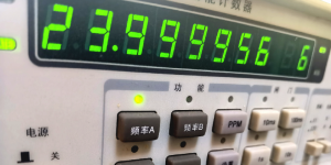
负载电容(CL) 负载电容(CL)是无源晶振的必选电气参数之一。关于该参数的选取,请严格遵循IC手册中晶振相关说明。 在振荡电路中,如果无源晶振两端的等效电容和标称负载电容存在差异,该晶振实际输出的频率将会与标称工作频率产生偏差,这种偏差被称之为“频率偏差”,简称“频偏”。这种偏差越小越好。 电容匹…时间:2023/03/03
晶振频偏主要原因之一:负载电容与电容匹配存在差异
负载电容(CL) 负载电容(CL)是无源晶振的必选电气参数之一。关于该参数的选取,请严格遵循IC手册中晶振相关说明。 在振荡电路中,如果无源晶振两端的等效电容和标称负载电容存在差异,该晶振实际输出的频率将会与标称工作频率产生偏差,这种偏差被称之为“频率偏差”,简称“频偏”。这种偏差越小越好。 电容匹…时间:2023/03/03 -
; ) 有源晶振的Tri-state/三态脚可以输入3.3V吗?
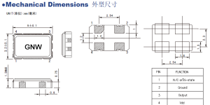
有源晶振的Tri-state/三态脚可以输入3.3V吗? 答:如果有源晶振的额定输入电压(Power Supply )为3.3V,Tri-state/三态脚可以输入3.3V。 一般情况下,有源晶振的1号脚若具备Tri-state/三态功能,指的是其本身增加了一个“开关”功能(与IC配合使用)。如果不…时间:2023/03/02
有源晶振的Tri-state/三态脚可以输入3.3V吗?
有源晶振的Tri-state/三态脚可以输入3.3V吗? 答:如果有源晶振的额定输入电压(Power Supply )为3.3V,Tri-state/三态脚可以输入3.3V。 一般情况下,有源晶振的1号脚若具备Tri-state/三态功能,指的是其本身增加了一个“开关”功能(与IC配合使用)。如果不…时间:2023/03/02
深圳市晶诺威科技有限公司