-
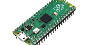; ) How to place the crystal oscillator on the PCB?
How to place the crystal oscillator on the PCB? Place the crystal oscillator as close as possible to the corresponding input and output pins of the ch…时间:2024/05/09

-
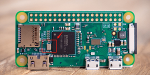; ) Crystal Oscillator PCB Layout Guidelines for Design
(Crystal Oscillator PCB Layout Guidelines for Design) When using a crystal oscillator in your PCB design, remember that it is very EMI sensitive and m…时间:2024/04/25
-
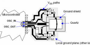; ) Layout issues of crystal oscillators
(Layout issues of crystal oscillators) Good layout practices are fundamental to the correct operation and reliability of the oscillator. It is critica…时间:2024/04/23
-
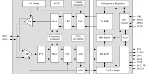; ) 无线高数据速率模式下晶振选型及布线注意事项
关于无线高数据速率模式下晶振选型及布线注意事项,晶诺威科技解释如下: 无线信号传输设备(如:蓝牙、Wi-Fi、ZigBee、Lora等)内部产生的频率都来自晶振所提供的频率(如:16MHz)。因此可以说,整个无线系统的性能主要取决于晶振参考频率的精度及稳定性。 对晶体振荡器的外部元器件应慎重选择,相…时间:2024/03/14
-
; ) 关于多层PCB设计中晶振接地(GND)问题
关于多层PCB设计中晶振接地(GND)问题,晶诺威科技解释如下: 在多层PCB设计中,合理的层叠设计有助于减小电磁干扰和信号干扰。通常,将信号层与地平面和电源平面隔开,有助于提高信号完整性和降低EMI。 地平面(Ground Plane) 指在电路设计中,用于连接和分布地(Ground)的导电区域。…时间:2024/01/17
-
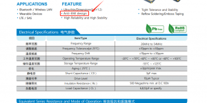; ) 关于抗电磁干扰(EMI)晶振的选择
抗电磁干扰(EMI)晶振 晶诺威科技针对电磁干扰(EMI)问题,研发了具有抗干扰特性的晶振。该类晶振通过采用特殊的电路设计、材料选择及制造工艺,有效提高了自身的抗电磁干扰能力。其输出频率具备高精度和高稳定度,因此可以为IC提供精准和稳定的参考时钟。 针对RF射频类电子产品,如蓝牙、WiFi等短距离无…时间:2023/12/25
-
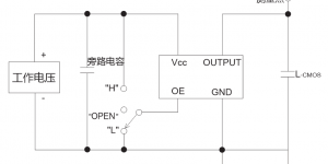; ) 如何消除有源晶振副波干扰?
如何消除有源晶振副波干扰?晶诺威科技解释如下: 1、 晶振外壳接地(通过接地引脚)设计,目的是防止晶振信号的向外辐射,同时屏蔽外来杂波干扰。 2、 晶振所在层铺地设计,目的是防止晶振信号干扰其它层。 3、 不要在电路板边缘设计安置晶振,以防止短路。 4、 若晶振位于电路板较边缘的位置,晶振与参考接地…时间:2023/10/07
-
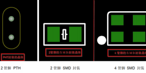; ) 晶振布线为何要加粗?
晶振布线为何要加粗? 答:减少晶振信号来自电路的干扰,因为电路过细,电阻会增大,电流会趋于不稳定,容易造成杂讯。 解释: 晶振线路加粗和尽量缩短与芯片之间距离是一个目的,就是减少信号电路中的阻抗及干扰,保障晶振频率信号传输后的精准性及稳定性。 电磁干扰对晶振性能的影响原因 1、电磁场中的电流感应:…时间:2023/08/24
-
Clock signal source and crystal oscillator时钟源与晶体振荡器
关于Clock signal source and crystal oscillator时钟源与晶体振荡器,晶诺威科技解释如下: Nowadays, almost all advanced microcontrollers use a crystal oscillator as their cloc…时间:2023/06/11
-
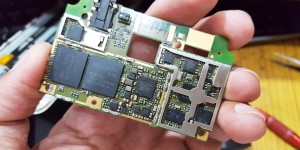; ) 关于晶体振荡器电路布线引发的问题(Layout Issues)
关于晶体振荡器电路布线引发的问题(Layout Issues),晶诺威科技解释如下: Good layout practices are fundamental to the correct operation and reliability of the oscillator. It is cri…时间:2023/06/06
深圳市晶诺威科技有限公司