
-
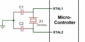
; ) 关于芯片对晶振电气参数要求的解释
关于芯片对晶振电气参数要求的解释如下: 举例: 某款蓝牙+WIFI控制器芯片,核心的射频和时钟系统是相同的,因此对晶振的要求也相同。 如下: 设计注意事项 如果产品需要在宽温度范围(如 -40℃ ~ +85℃)下稳定工作,请务必选择温度频差(Frequency versus Temperature …时间:2026/07/12
关于芯片对晶振电气参数要求的解释
关于芯片对晶振电气参数要求的解释如下: 举例: 某款蓝牙+WIFI控制器芯片,核心的射频和时钟系统是相同的,因此对晶振的要求也相同。 如下: 设计注意事项 如果产品需要在宽温度范围(如 -40℃ ~ +85℃)下稳定工作,请务必选择温度频差(Frequency versus Temperature …时间:2026/07/12
-
; ) 晶振信号输入输出走线可以换层(layer)吗?
晶振信号输入输出走线可以换层(layer)吗? 答:对于晶振信号的输入输出走线,原则上建议尽量避免换层,但在特定条件下可以换层,前提是做好充分的信号完整性(SI)与电磁兼容(EMC)设计。换句话说,设计时将晶振与芯片放在PCB同一面(通常TOP层),保持走线直线、平行、等长、极短(<12mm,…时间:2026/07/06
晶振信号输入输出走线可以换层(layer)吗?
晶振信号输入输出走线可以换层(layer)吗? 答:对于晶振信号的输入输出走线,原则上建议尽量避免换层,但在特定条件下可以换层,前提是做好充分的信号完整性(SI)与电磁兼容(EMC)设计。换句话说,设计时将晶振与芯片放在PCB同一面(通常TOP层),保持走线直线、平行、等长、极短(<12mm,…时间:2026/07/06 -
; ) 关于晶振走线和信号线需要注意的几点建议
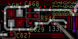
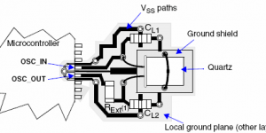
晶振走线(连接晶振两端的线)本身是关键的高频小信号线,布线时需要特别注意。 核心原则可以总结为: 晶振下方的区域以及其走线,应被视为一个独立的敏感模拟区,与其它数字信号线(如 I2C、SPI、UART、GPIO)进行物理隔离。 下面是具体的对比和规则: 1、 晶振走线的自身要求 尽量短: 晶振应紧邻…时间:2026/07/01
关于晶振走线和信号线需要注意的几点建议
晶振走线(连接晶振两端的线)本身是关键的高频小信号线,布线时需要特别注意。 核心原则可以总结为: 晶振下方的区域以及其走线,应被视为一个独立的敏感模拟区,与其它数字信号线(如 I2C、SPI、UART、GPIO)进行物理隔离。 下面是具体的对比和规则: 1、 晶振走线的自身要求 尽量短: 晶振应紧邻…时间:2026/07/01 -
; ) 无源晶振及电容如何布板?
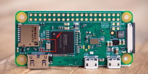
关于无源晶振及电容如何布板,晶诺威科技建议如下: 无源晶振的PCB布局,核心是要做到三点:近、短、净。即把晶振和电容尽量靠近芯片、走线尽量短、并做好屏蔽保护。 下面是具体的操作要点: 1、布局要点 优先固定晶振位置: 将晶振本体紧邻MCU的时钟引脚(如OSC_IN/OSC_OUT)放置,间距最好控制…时间:2026/05/21
无源晶振及电容如何布板?
关于无源晶振及电容如何布板,晶诺威科技建议如下: 无源晶振的PCB布局,核心是要做到三点:近、短、净。即把晶振和电容尽量靠近芯片、走线尽量短、并做好屏蔽保护。 下面是具体的操作要点: 1、布局要点 优先固定晶振位置: 将晶振本体紧邻MCU的时钟引脚(如OSC_IN/OSC_OUT)放置,间距最好控制…时间:2026/05/21 -
; ) 关于SMD3225晶振布线说明
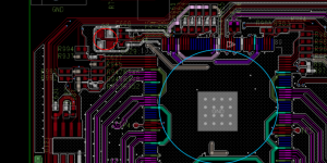
关于SMD3225晶振布线设计,晶诺威科技说明如下: SMD3225晶振是一种表面贴装(SMD)封装的石英晶体振荡器,尺寸为3.2mm × 2.5mm。它在高频电路中广泛应用,如通信设备、消费电子和工业控制等。为了确保SMD3225晶振的正常工作和稳定性,PCB布线设计非常关键。以下是SMD3225…时间:2025/04/18
关于SMD3225晶振布线说明
关于SMD3225晶振布线设计,晶诺威科技说明如下: SMD3225晶振是一种表面贴装(SMD)封装的石英晶体振荡器,尺寸为3.2mm × 2.5mm。它在高频电路中广泛应用,如通信设备、消费电子和工业控制等。为了确保SMD3225晶振的正常工作和稳定性,PCB布线设计非常关键。以下是SMD3225…时间:2025/04/18 -
; ) 信号线到晶振的距离是多少?
信号线到晶振的距离是多少? 答:距离越短越好,通常不超过5厘米,高频应用需更短。 信号线到晶振的距离应尽可能短,以减少噪声和信号完整性问题。晶诺威科技具体建议如下: 一般建议: 距离最好控制在 5厘米 以内。 高频应用: 在高频电路中,距离应进一步缩短,通常小于 2.5厘米。 布局优化: 信号线应直…时间:2025/04/10
信号线到晶振的距离是多少?
信号线到晶振的距离是多少? 答:距离越短越好,通常不超过5厘米,高频应用需更短。 信号线到晶振的距离应尽可能短,以减少噪声和信号完整性问题。晶诺威科技具体建议如下: 一般建议: 距离最好控制在 5厘米 以内。 高频应用: 在高频电路中,距离应进一步缩短,通常小于 2.5厘米。 布局优化: 信号线应直…时间:2025/04/10 -
; ) How to place the crystal oscillator on the PCB?
How to place the crystal oscillator on the PCB? Place the crystal oscillator as close as possible to the corresponding input and output pins of the ch…时间:2024/05/09
How to place the crystal oscillator on the PCB?
How to place the crystal oscillator on the PCB? Place the crystal oscillator as close as possible to the corresponding input and output pins of the ch…时间:2024/05/09 -
; ) Crystal Oscillator PCB Layout Guidelines for Design
(Crystal Oscillator PCB Layout Guidelines for Design) When using a crystal oscillator in your PCB design, remember that it is very EMI sensitive and m…时间:2024/04/25
Crystal Oscillator PCB Layout Guidelines for Design
(Crystal Oscillator PCB Layout Guidelines for Design) When using a crystal oscillator in your PCB design, remember that it is very EMI sensitive and m…时间:2024/04/25 -
; ) Layout issues of crystal oscillators
(Layout issues of crystal oscillators) Good layout practices are fundamental to the correct operation and reliability of the oscillator. It is critica…时间:2024/04/23
Layout issues of crystal oscillators
(Layout issues of crystal oscillators) Good layout practices are fundamental to the correct operation and reliability of the oscillator. It is critica…时间:2024/04/23 -
; ) 关于晶体振荡器电路布线引发的问题(Layout Issues)
关于晶体振荡器电路布线引发的问题(Layout Issues),晶诺威科技解释如下: Good layout practices are fundamental to the correct operation and reliability of the oscillator. It is cri…时间:2023/06/06
关于晶体振荡器电路布线引发的问题(Layout Issues)
关于晶体振荡器电路布线引发的问题(Layout Issues),晶诺威科技解释如下: Good layout practices are fundamental to the correct operation and reliability of the oscillator. It is cri…时间:2023/06/06